- 您现在的位置:买卖IC网 > Sheet目录473 > MAX2852ITK+ (Maxim Integrated)IC RECEIVER DFS 5GHZ 68TQFN
�� �
�
�5GHz� Receiver�
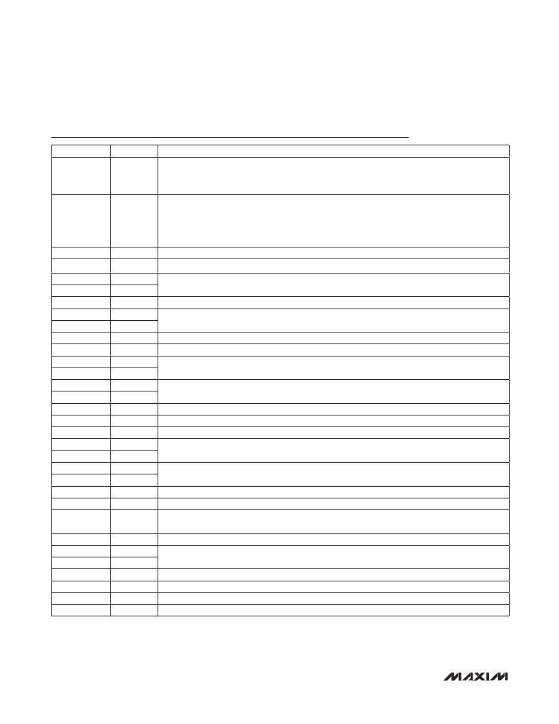
�Pin� Description�
�PIN�
�1,� 2,� 5,� 6,� 9,�
�10,� 12,� 13,�
�16,� 66,� 67�
�3,� 8,� 11,� 14,�
�19,� 22,�
�35–38,� 54,�
�56–59,� 61–65,�
�68�
�4,� 7,� 15,� 18�
�17�
�20�
�21�
�23�
�24�
�25�
�26�
�27�
�28�
�29�
�30�
�31�
�32�
�33�
�34�
�39�
�40�
�41�
�42�
�43�
�44�
�45�
�46�
�47�
�48�
�49�
�50�
�51�
�52�
�NAME�
�V� CC�
�N.C.�
�GND�
�V� CC_UCX�
�TXRF-�
�TXRF+�
�V� CC_LNA�
�RXRF-�
�RXRF+�
�V� CC_MXR�
�V� CC_BB2�
�TXBBI+�
�TXBBI-�
�TXBBQ+�
�TXBBQ-�
�CS�
�SCLK�
�DIN�
�RXBBI+�
�RXBBI-�
�RXBBQ+�
�RXBBQ-�
�RSSI�
�V� CC_VCO�
�BYP_VCO�
�GND_VCO�
�CPOUT+�
�CPOUT-�
�V� CC_DIG�
�DOUT�
�CLKOUT�
�V� CC_XTAL�
�FUNCTION�
�Supply� Voltage�
�No� Connection�
�Ground�
�Transmitter Upconverter Supply Voltage. Bypass with a capacitor as close as possible to the pin.�
�Transmitter� Differential� Outputs.� These� pins� are� in� open-collector� configuration.� They� hould� be�
�biased� at� supply� voltage� with� differential� impedance� terminated� at� 300� W� .�
�Receiver� LNA� Supply� Voltage.� Bypass� with� a� capacitor� as� close� as� possible� to� the� pin.�
�Receiver� LNA� Differential� Inputs.� Inputs� are� DC-coupled� and� biased� internally� at� 1.2V.�
�Receiver Downconverter Supply Voltage. Bypass with a capacitor as close as possible to the pin.�
�Receiver� Baseband� Supply� Voltage� 2.� Bypass� with� a� capacitor� as� close� as� possible� to� the� pin.�
�Transmitter� Baseband� I-Channel� Differential� Inputs�
�Transmitter� Baseband� Q-Channel� Differential� Inputs�
�Chip-Select� Logic� Input� of� 4-Wire� Serial� Interface�
�Serial-Clock� Logic� Input� of� 4-Wire� Serial� Interface�
�Data� Logic� Input� of� 4-Wire� Serial� Interface�
�Receiver� Baseband� I-Channel� Differential� Outputs�
�Receiver� Baseband� Q-Channel� Differential� Outputs�
�Receiver� Signal� Strength� Indicator� Output�
�VCO� Supply� Voltage.� Bypass� with� a� capacitor� as� close� as� possible� to� the� pin.�
�On-Chip� VCO� Regulator� Output� Bypass.� Bypass� with� an� external� 1� F� F� capacitor� to� GND_VCO�
�with� minimum� PCB� trace.� Do� not� connect� other� circuitry� to� this� pin.�
�VCO� Ground�
�Differential� Charge-Pump� Outputs.� Connect� the� frequency� synthesizer’s� loop� filter� between�
�CPOUT+� and� CPOUT-� (see� the� Typical� Operating� Circuit� ).�
�Digital� Block� Supply� Voltage.� Bypass� with� a� capacitor� as� close� as� possible� to� the� pin.�
�Data� Logic� Output� of� 4-Wire� Serial� Interface�
�Reference� Clock� Buffer� Output�
�Crystal� Oscillator� Supply� Voltage.� Bypass� with� a� capacitor� as� close� as� possible� to� the� pin.�
�16�
�_____________________________________________________________________________________�
�发布紧急采购,3分钟左右您将得到回复。
相关PDF资料
MAX2870EVKIT#
EVAL KIT MAX2870
MAX2904EVKIT
EVAL KIT
MAX3524EVKIT
EVAL KIT MAX3524
MAX3540EVKIT#
KIT FOR MAX3540 DVB TUNER
MAX3541EVKIT+
KIT FOR MAX3541 DVB TUNER
MAX3542CLM+
IC TV TUNER SGL CONV 48LFCGA
MAX3542EVKIT+
KIT FOR MAX3542 DVB TUNER
MAX3543EVKIT+
EVAL KIT MAX3543
相关代理商/技术参数
MAX2852ITK+T
功能描述:射频接收器 5Ghz Receiver RoHS:否 制造商:Skyworks Solutions, Inc. 类型:GPS Receiver 封装 / 箱体:QFN-24 工作频率:4.092 MHz 工作电源电压:3.3 V 封装:Reel
MAX2870ETJ+
功能描述:锁相环 - PLL PLL/VCO RoHS:否 制造商:Silicon Labs 类型:PLL Clock Multiplier 电路数量:1 最大输入频率:710 MHz 最小输入频率:0.002 MHz 输出频率范围:0.002 MHz to 808 MHz 电源电压-最大:3.63 V 电源电压-最小:1.71 V 最大工作温度:+ 85 C 最小工作温度:- 40 C 封装 / 箱体:QFN-36 封装:Tray
MAX2870ETJ+T
功能描述:锁相环 - PLL PLL/VCO RoHS:否 制造商:Silicon Labs 类型:PLL Clock Multiplier 电路数量:1 最大输入频率:710 MHz 最小输入频率:0.002 MHz 输出频率范围:0.002 MHz to 808 MHz 电源电压-最大:3.63 V 电源电压-最小:1.71 V 最大工作温度:+ 85 C 最小工作温度:- 40 C 封装 / 箱体:QFN-36 封装:Tray
MAX2870EVKIT#
功能描述:射频开发工具 MAX2870 Eval Kit RoHS:否 制造商:Taiyo Yuden 产品:Wireless Modules 类型:Wireless Audio 工具用于评估:WYSAAVDX7 频率: 工作电源电压:3.4 V to 5.5 V
MAX2880ETP+
制造商:Maxim Integrated Products 功能描述:12.4GHZ HIGH PERFORMANCE FRACTIONAL/INTEGER-N SYNTHESIZER - Rail/Tube 制造商:Maxim Integrated Products 功能描述:RF FRACT INTEGER N SYNTH QFN
MAX2880ETP+T
制造商:Maxim Integrated Products 功能描述:RF FRACT INTEGER N SYNTH QFN
MAX2900EGI
功能描述:射频发射器 RoHS:否 制造商:Micrel 类型:ASK Transmitter 封装 / 箱体:SOT-23-6 工作频率:300 MHz to 450 MHz 封装:Reel
MAX2900EGI-BOW
功能描述:射频发射器 RoHS:否 制造商:Micrel 类型:ASK Transmitter 封装 / 箱体:SOT-23-6 工作频率:300 MHz to 450 MHz 封装:Reel